
New research has demonstrated that the secrets of the tiniest active structures in integrated circuits can be revealed using a non-destructive imaging technique. The breakthrough required the efforts of an international team of scientists from JKU and Keysight Technologies (Austria), ETH/EPFL/PSI and IBM Research – Europe (Switzerland) and from UCL (UK).
The life-givers of integrated circuits and quantum devices in silicon are small structures made from patches of foreign atoms called dopants. The dopant structures provide charge carriers that flow through the components of the circuit, giving the components their ability to function. These days the dopant structures are only a few atoms across and so need to be made in precise locations within a circuit and have very well-defined electrical properties. At present manufacturers find it hard to tell in a non-destructive way whether they have made their devices according to these strict requirements. A new imaging paradigm promises to change all that.
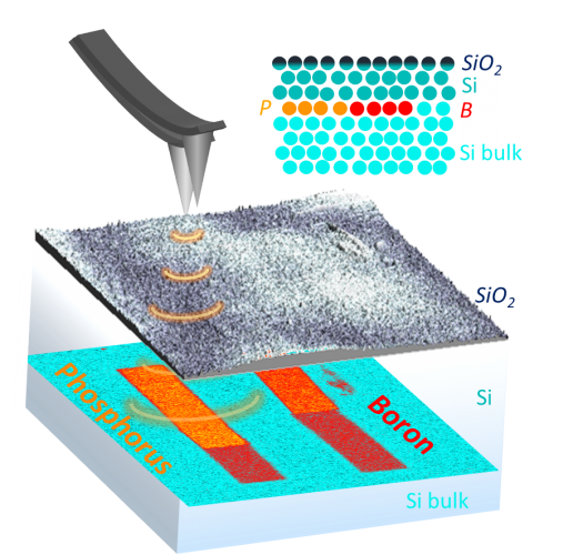
The imaging mode called broadband electric force microscopy, developed by Dr Georg Gramse at Keysight technologies & JKU uses a very sharp probe that sends electromagnetic waves into a silicon chip, to image and localize dopant structures underneath the surface. Dr Gramse says that because the microscope can use waves with many frequencies it can provide a wealth of previously inaccessible detail about the electrical environment around the dopant structures. The extra information is crucial to predicting how well the devices will ultimately perform.
The imaging approach was tested on two tiny dopant structures made with a templating process which is unique in achieving atomically sharp interfaces between differently doped regions. Dr Tomas Skeren at IBM produced the world’s first electronic diode (a circuit component which passes current in only one direction) fabricated with this templating process, while Dr Alex Kölker at UCL created a multilevel 3-D device with atomic scale precision.
The results, published in the journal Nature Electronics, demonstrate that the technique can take pictures and resolve as few as 200 dopant atoms even if they are hidden below the same number of Si atoms. It can tell the difference between certain flavours of dopant atoms, and can also provide information about the way charge carriers move through the structures and about atomic-sized ‘traps’ that can stop them from moving.
According to Professor Neil Curson, who leads the group at UCL “This research could not have come at a better time for the massive world-wide effort to make smaller electronics or quantum computers in silicon. While the success in making components smaller and more complicated has been spectacular, the technology required to actually observe what is being made has not been keeping up. This has become a major problem for quality control in silicon chip manufacture and for information security, when you can’t see what’s inside the chips you are making or buying. Our new research will help solve many of these issues.”
Dr. Andreas Fuhrer from IBM Research points out “After learning to make the first tiny dopant device structures consisting of two different dopant species, boron and phosphorous, it was extremely useful to work with this international team to discover subtle details about our structures that would just not be possible in any other way.”
The full article is available to read in Nature Electronics, Nanoscale imaging of mobile carriers and trapped charges in delta doped silicon p–n junctions. Georg Gramse , Alexander Kölker, Tomáš Škereň, Taylor J. Z. Stock , Gabriel Aeppli, Ferry Kienberger, Andreas Fuhrer and Neil J. Curson
Additional Links